bez PVN
ar PVN

Meklējiet produktu, ražotāja kodu vai ražotāju
Detaļu saraksts
Pieteikties/Reģistrēties
0.00(bez PVN)


Tehniskie Dokumenti
Specifikācija
Brand
Renesas ElectronicsProduct Type
Clock Buffer
Maximum Input Frequency
200MHz
Maximum Propagation Delay Time
350ps
Mount Type
Surface
Package Type
SOIC
Pin Count
8
Minimum Supply Voltage
3V
Maximum Supply Voltage
4.6V
Minimum Operating Temperature
-40°C
Maximum Operating Temperature
85°C
Standards/Approvals
No
Series
IDT23S05E
Automotive Standard
No
Izcelsmes valsts
Philippines
Produkta Apraksts
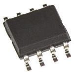
The Renesas Electronics zero delay clock buffer is a high-speed phase-lock loop (PLL) clock buffer, designed to address high-speed clock distribution applications. The zero delay is achieved by aligning the phase between the incoming clock and the output clock, operable within the range of 10 to 200MHz. The PLL feedback is on-chip and is obtained from the CLKOUT pad. In the absence of an input clock, it enters power down.

Ideate. Create. Collaborate
JOIN FOR FREE
No hidden fees!


Noliktavas stāvoklis patreiz nav pieejams
€ 7,70
€ 0,77 Katrs (tiek piegadats Tubina) (bez PVN)
€ 9,32
€ 0,932 Katrs (tiek piegadats Tubina) (Ieskaitot PVN)
Industriālais iepakojums (Penālis)
10
€ 7,70
€ 0,77 Katrs (tiek piegadats Tubina) (bez PVN)
€ 9,32
€ 0,932 Katrs (tiek piegadats Tubina) (Ieskaitot PVN)
Noliktavas stāvoklis patreiz nav pieejams
Industriālais iepakojums (Penālis)
10
| Daudzums | Vienības cena | Per Penālis |
|---|---|---|
| 10 - 20 | € 0,77 | € 3,85 |
| 25 - 45 | € 0,73 | € 3,65 |
| 50 - 90 | € 0,714 | € 3,57 |
| 95+ | € 0,702 | € 3,51 |
Ideate. Create. Collaborate
JOIN FOR FREE
No hidden fees!
Tehniskie Dokumenti
Specifikācija
Brand
Renesas ElectronicsProduct Type
Clock Buffer
Maximum Input Frequency
200MHz
Maximum Propagation Delay Time
350ps
Mount Type
Surface
Package Type
SOIC
Pin Count
8
Minimum Supply Voltage
3V
Maximum Supply Voltage
4.6V
Minimum Operating Temperature
-40°C
Maximum Operating Temperature
85°C
Standards/Approvals
No
Series
IDT23S05E
Automotive Standard
No
Izcelsmes valsts
Philippines
Produkta Apraksts
The Renesas Electronics zero delay clock buffer is a high-speed phase-lock loop (PLL) clock buffer, designed to address high-speed clock distribution applications. The zero delay is achieved by aligning the phase between the incoming clock and the output clock, operable within the range of 10 to 200MHz. The PLL feedback is on-chip and is obtained from the CLKOUT pad. In the absence of an input clock, it enters power down.
Ideate. Create. Collaborate
JOIN FOR FREE
No hidden fees!