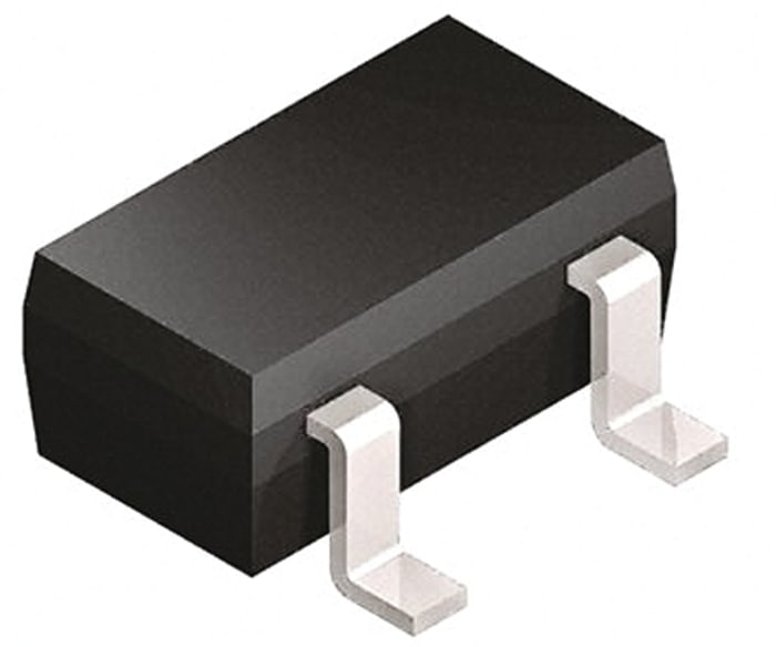
P-Channel MOSFET Transistor, 1.18 A, 20 V, 3-Pin SOT-23 Infineon BSS215P

Tehniskie dokumenti
Specifikācija
Brand
InfineonChannel Type
P
Maximum Continuous Drain Current
1.18 A
Maximum Drain Source Voltage
20 V
Package Type
SOT-23
Mounting Type
Surface Mount
Pin Count
3
Maximum Drain Source Resistance
280 mΩ
Channel Mode
Enhancement
Maximum Power Dissipation
500 mW
Maximum Gate Source Voltage
-12 V, +12 V
Maximum Operating Temperature
+150 °C
Length
2.9mm
Typical Gate Charge @ Vgs
3.6 nC @ 4.5 V
Width
1.3mm
Number of Elements per Chip
1
Minimum Operating Temperature
-55 °C
Height
1mm
Izcelsmes valsts
China
Ideate. Create. Collaborate
JOIN FOR FREE
No hidden fees!


- Download and use our DesignSpark software for your PCB and 3D Mechanical designs
- View and contribute website content and forums
- Download 3D Models, Schematics and Footprints from more than a million products
P.O.A.
Katrs (Paka ir 50) (bez PVN)
50
P.O.A.
Katrs (Paka ir 50) (bez PVN)
Noliktavas stāvoklis patreiz nav pieejams
50
Noliktavas stāvoklis patreiz nav pieejams
Ideate. Create. Collaborate
JOIN FOR FREE
No hidden fees!
- Download and use our DesignSpark software for your PCB and 3D Mechanical designs
- View and contribute website content and forums
- Download 3D Models, Schematics and Footprints from more than a million products
Tehniskie dokumenti
Specifikācija
Brand
InfineonChannel Type
P
Maximum Continuous Drain Current
1.18 A
Maximum Drain Source Voltage
20 V
Package Type
SOT-23
Mounting Type
Surface Mount
Pin Count
3
Maximum Drain Source Resistance
280 mΩ
Channel Mode
Enhancement
Maximum Power Dissipation
500 mW
Maximum Gate Source Voltage
-12 V, +12 V
Maximum Operating Temperature
+150 °C
Length
2.9mm
Typical Gate Charge @ Vgs
3.6 nC @ 4.5 V
Width
1.3mm
Number of Elements per Chip
1
Minimum Operating Temperature
-55 °C
Height
1mm
Izcelsmes valsts
China
Ideate. Create. Collaborate
JOIN FOR FREE
No hidden fees!
- Download and use our DesignSpark software for your PCB and 3D Mechanical designs
- View and contribute website content and forums
- Download 3D Models, Schematics and Footprints from more than a million products